Business description
- HOME
- Business description
- New Business
New Business
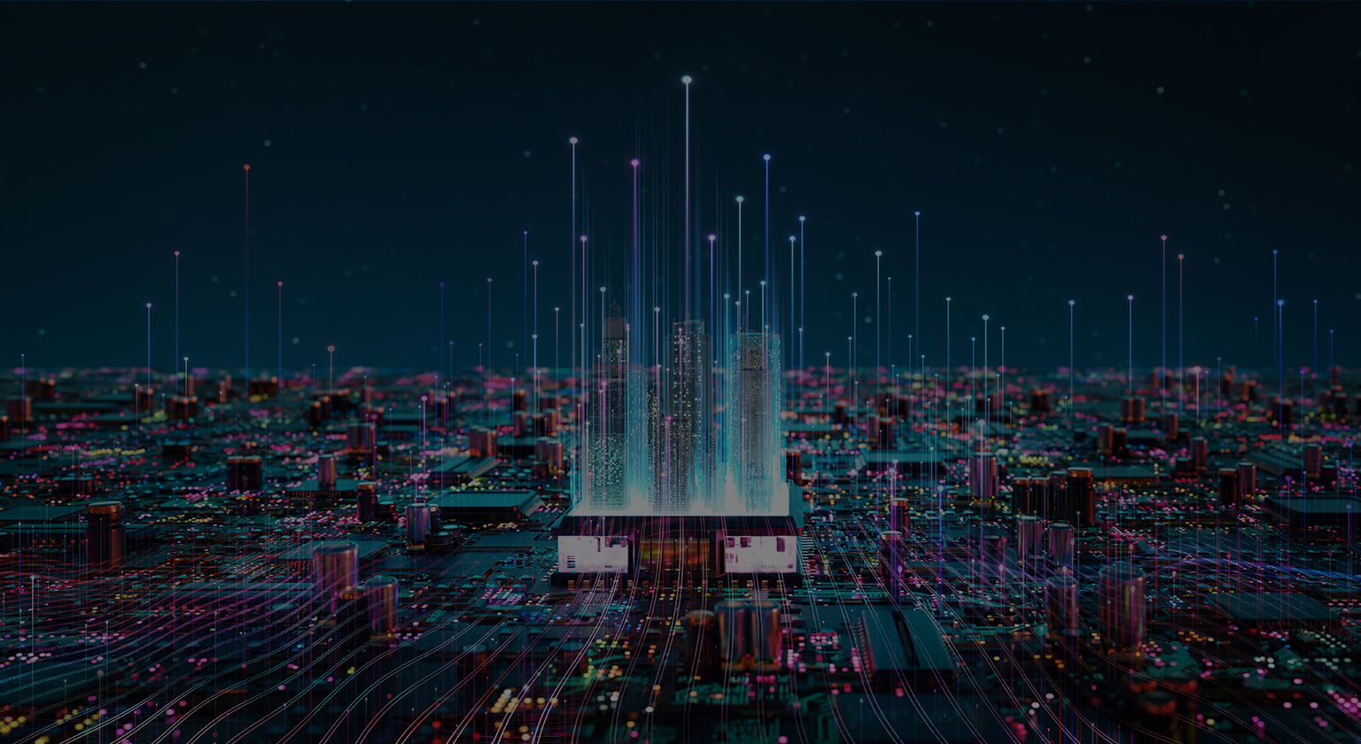
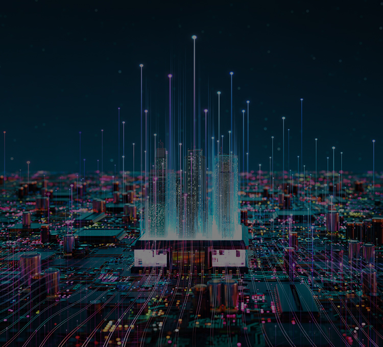
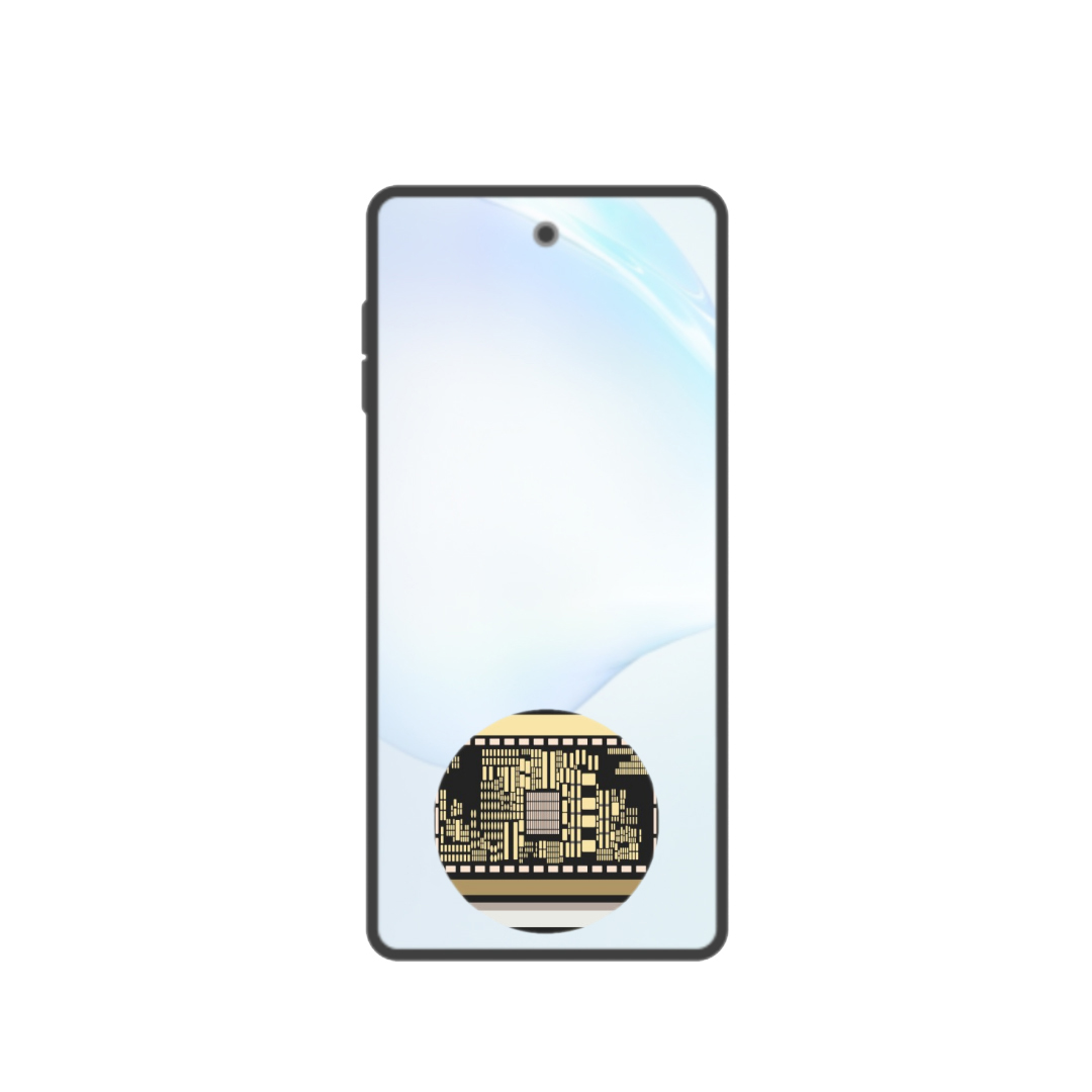
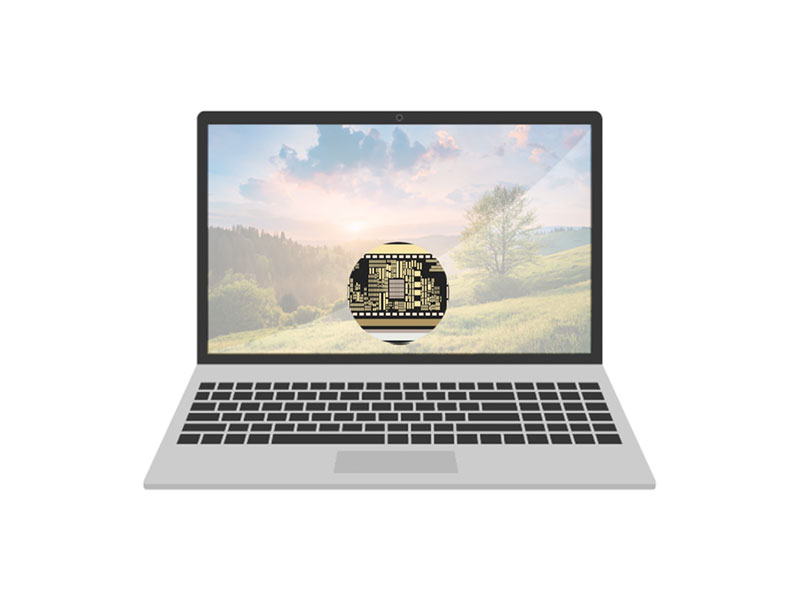
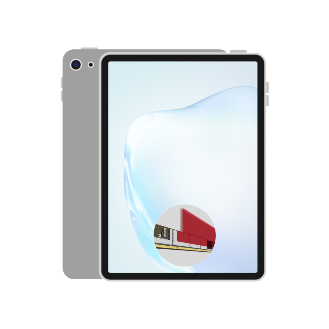
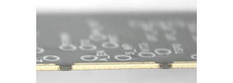
BH PCBs are main boards that better integrate top technologies such as high density layer, fine pattern, and micro via compared to general PCBs, supporting high functionalization of electronic devices such as smart phones and tablet PCs.
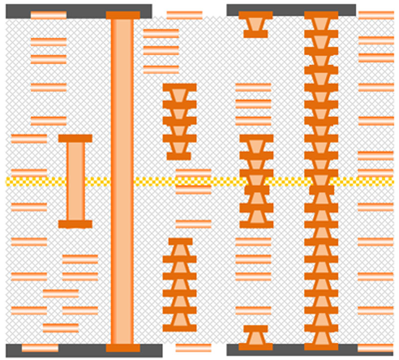
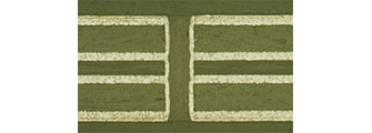
Structure


Features and benefits
- Optimized vertical routing solution in one compact structure.
- Simplifies trace routes between multiple layers.
- Provides efficient connectivity integration for high-density PCBs by offering a compressed footprint and multi-layer reach
- Via fill electrification provides superior reliability and electrical characteristics
- Registered technology to prevent LVH tilting on each layer and ensure the high reliability required to prevent interfacial detachment.
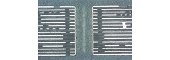
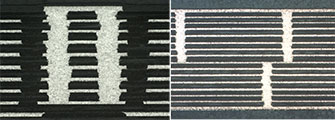
- Using BITs to machine PTH on the same point requires high machining precision.
- Minimizes signal loss by forming an even electroplating layer.
- High Aspect Ratio enables high capacity data transmission.
- Prevents electromagnetic waves from being emitted or leaked to the edge of the board.
- Improves PCB EMC performance.
- Provides superior signal integrity.
- Heat dissipation and cooling.
- Increases current carrying capacity.
- Fill inner via holes with resin to ensure reliability against failure regarding shrinkage and expansion.
- Integrated pad and via hole area for mounting elements.
Detailed specifications
| Specification | |
|---|---|
| No. of Layers | 4~20L |
| Base Material(Laminate) | FR-4, High Tg FR-4, Halogen Free |
| Base Material(Build up) | FR-4, RCC, High Tg FR-4, Halogen Free, etc |
| Board Thickness | 0.3~1.6T |
| Min.Line Width | 30um |
| Min Line Spacing | 40um |
| Min. Mech. Drill Size | 150um |
| Min. Laser. Drill Size | 80um |
| Surface Treatment | ENIG, Immersion TIN, Selectve OSP |
| Comment | Stack via, Staggered via, Filled via |
| Type | PCS & KIT |
25, Pyeongcheon-ro 199beon-gil, Bupyeong-gu, Incheon (Cheongcheon-dong) TEL : 032.510.2000 | FAX : 032-514-8677 | E-mail : bhflex@bhflex.co.kr | R&D inquiry : technology@bhflex.co.kr | BH Cyber Shinmungo : bhjebo@naver.com
Copyright 2017 bhflex Co. Ltd. ALL RIGHTS RESERVED
25, Pyeongcheon-ro 199beon-gil, Bupyeong-gu, Incheon (Cheongcheon-dong)
TEL : 032.510.2000
FAX : 032-514-8677 | E-mail : bhflex@bhflex.co.kr
R&D inquiry : technology@bhflex.co.kr
BH Cyber Shinmungo : bhjebo@naver.com