

R&D
- HOME
- R&D
- R&D information
- Technology
Technology
''BH, a leading R&D organization preparing for the future,
is leading the creation of new values through ceaseless efforts and investments.'
BH's R&D researchers are specialized in new product development/mass production with their leading technology,,
and strive to improve BH's products and services.
Via Hole
Technology
Fine Pattern
Technology
Surface Insulation
Technology
ACF Reliability
Development of automatic punching machine
Landless
Technology
Micro LED
Technology
Stretchable FPCB
Technology
Via Hole Technology
- Realization of high integration of wiring, minimization of signal loss, and improvement of thermal reliability through various interlayer conduction technology
- Able to propose customized technology for each product group
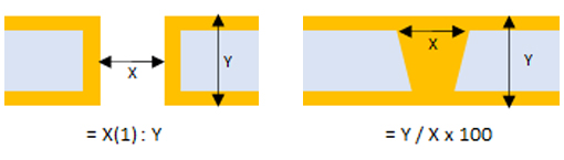
| Normal | |||||
|---|---|---|---|---|---|
| Mechanical Drill Normal Plating | Laser Via hole Normal Plating | Laser Via & Via on Via Via Fill Plating | |||
 |
|
 |
|
 |
|
| Special | |||||
| Though Hole Via Filling | Ultra Micro Via Normal & Via Filling | ||||
 |
|
 |
|
||
| Normal | |
|---|---|
| Mechanical Drill Normal Plating | |
|
|
| Laser Via hole Normal Plating | |
|
|
| Laser Via & Via on Via Via Fill Plating | |
|
|
| Special | |
| Though Hole Via Filling | |
|
|
| Ultra Micro Via Normal & Via Filling | |
|
|
※ Aspect Ratio
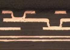
Fine Pattern Technology
- Implementation of Fine Pattern according to high functionality needs
- Light, thin, short and small due to increased design freedom
| Mass production level |
|---|
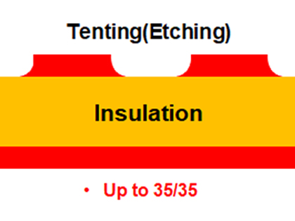 |
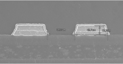
[ Tenting (Etching Process) ] |
|
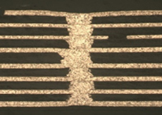
| R&D |
|---|
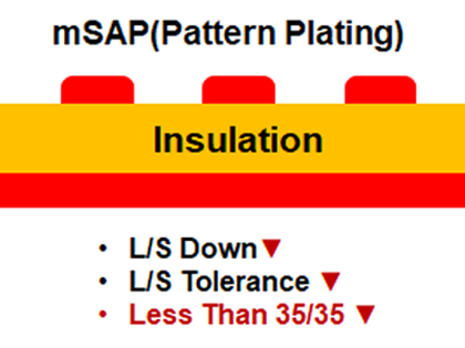 |
[ mSAP ( Modified Semi-additive Process) ] |
|
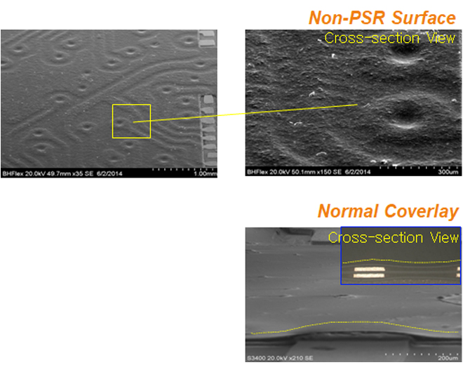
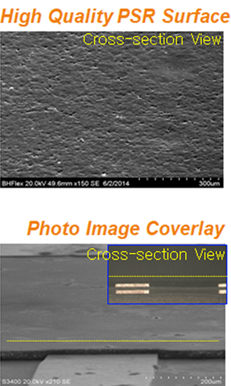
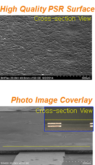
Surface Insulation Technology
- Development of solder mask and insulation surface finishing method
- Able to implement high-flatness
- Improved solderability and wire bondability
- Main applications: Camera module, Sensor mounting application.
 |
|
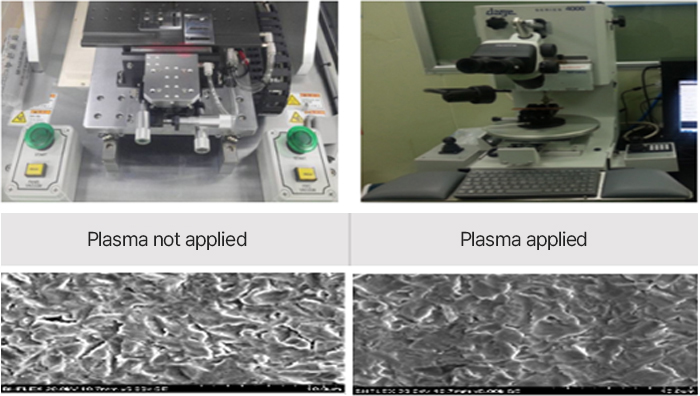
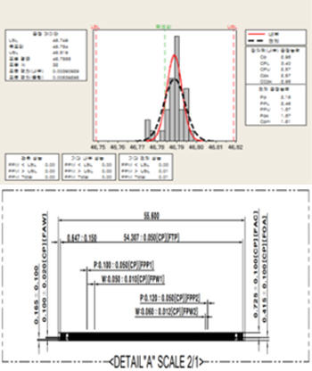
ACF Reliability
- ACF tension → Parameter optimization/ quality assurance system
- ACF (OLB) terminal elongation optimization → ±0.05mm (cpk 1.33 ▲)
- RTR/sheet input scale optimization → minimization scale deviation for each facility
| ACF Bonder / PEEL / Plasma | Elongation management |
|---|---|
 |
 |
| ACF Bonder / PEEL / Plasma |
|---|
|
| Elongation management |
|
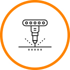
Development of automatic punching machine
- Automatic input + sorting + automatic punching + discharge automation → defective handling rate ▼
- Punching + sorting Merge → Open, Short sorting loading
| Facility floor plan | Facility Flow | |||
|---|---|---|---|---|
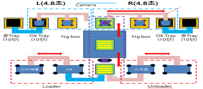 |
 Automatic input |
 Automatic punching |
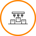 Automatic sorting |
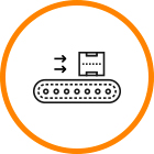 Automatic discharge |
| Facility floor plan | |||
|---|---|---|---|
|
|||
| Facility Flow | |||
Automatic input |
Automatic punching |
Automatic sorting |
Automatic discharge |
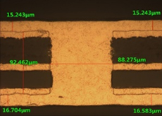
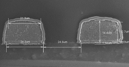
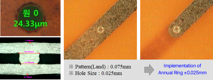
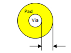
Landless Technology
- Able to implement landless through reduction of hole annual ring in addition to Ultra Micro Via Hole technology
- R&D Technology: Implementation of Annual Ring ±25um
- Landless Effect: Improved design freedom
| Mass production level | |
|---|---|
 |
|
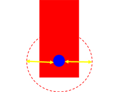
| Land | 300㎛ |
| Via | 100㎛ |


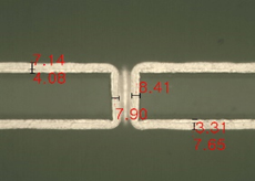
| Mass production level | |
|---|---|
 |
|
| Land | 75㎛ |
| Via | 25㎛ |

| BH R&D Technology : Landless FPC |
|---|
 |
Micro LED Technology
- Development of Micro LED to express complete black color, which is difficult to implement in the existing Back Light LCD Display → Existing LCD Backlight LCD Displays have a phenomenon in which light appears to be spread due to backlight interference nearby
- Micro LED Design & BH FPCB Technology
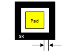
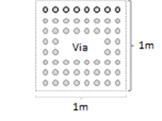
| Classification | Fine Pattern Min Line/Space(um) | Small Via & Pad Annual Ring(um) | SR Tolerance Eccentric Tolerance (um) | a lot of Via Hole Number of Holes (EA/sqm) |
|---|---|---|---|---|
| Normal Application | 45/45 | 100 | 40 | 10~30만 |
| Micro LED | 35/35↓ | 30↓ | 20 | 100↑ |
| ETC |  |
 |
 |
 |
| Classification | Fine Pattern Min Line/Space(um) | Small Via & Pad Annual Ring(um) |
|---|---|---|
| Normal Application | 45/45 | 100 |
| Micro LED | 35/35↓ | 30↓ |
| ETC | |
|
| Classification | SR Tolerance Eccentric Tolerance (um) | a lot of Via Hole Number of Holes (EA/sqm) |
| Normal Application | 40 | 10~30만 |
| Micro LED | 20 | 100↑ |
| ETC | |
|
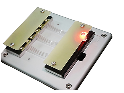
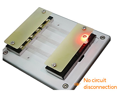
Stretchable FPCB Technology
- Development of Stretchable FPCB capable of mechanical wiring such as curved surfaces or spheres
- Applicable to products requiring repetition and extension
- Able to suppress disconnection due to increased resistance caused by stretching and deformation / increased fatigue strength
| Stretchable Test | |
|---|---|
 |
 |
25, Pyeongcheon-ro 199beon-gil, Bupyeong-gu, Incheon (Cheongcheon-dong) TEL : 032.510.2000 | FAX : 032-514-8677 | E-mail : bhflex@bhflex.co.kr | R&D inquiry : technology@bhflex.co.kr | BH Cyber Shinmungo : bhjebo@naver.com
Copyright 2017 bhflex Co. Ltd. ALL RIGHTS RESERVED
25, Pyeongcheon-ro 199beon-gil, Bupyeong-gu, Incheon (Cheongcheon-dong)
TEL : 032.510.2000
FAX : 032-514-8677 | E-mail : bhflex@bhflex.co.kr
R&D inquiry : technology@bhflex.co.kr
BH Cyber Shinmungo : bhjebo@naver.com